
Robert Wachen, the co-founder and COO of Etched, represents a new wave of silicon pioneers who dared to challenge the dominance of general-purpose hardware. Along with his co-founders, he walked away from a prestigious path at Harvard in 2022 to pursue a vision that many in the tech industry dismissed as “wacky”: building specialized chips tailored specifically for the transformer architecture that powers today’s generative AI. Today, Etched stands as a burgeoning titan in the hardware space, recently securing a $300 million Series C round that skyrocketed the company’s valuation to a staggering $10.3 billion. In this conversation, we explore the grueling journey from a makeshift garage setup to managing massive data centers and the technical breakthroughs that have already secured $1 billion in advance orders from some of the world’s largest AI developers.
The transition from the academic halls of Harvard to the gritty reality of a startup was a profound shock to the system, involving everything from sleeping on floors to managing rudimentary hardware setups. This journey was defined by a relentless focus on the “transformer” architecture, a choice that doubled the company’s valuation from $5 billion to over $10 billion in just seven months. We discuss the technical nuances of their prefill and decode chips, the efficiency of low-voltage inference, and the massive operational leap from a small lab to an 80,000-square-foot facility.
You walked away from an Ivy League education to launch a hardware startup during a period of massive uncertainty, eventually finding yourself sleeping on a friend’s floor in the Bay Area. Looking back at those early days in the garage, what was the most grounding moment that made you realize the sheer scale of the challenge you had taken on?
The reality of our situation hit me hardest when I was sleeping on the floor of a friend’s house they were about to sell, using a thin towel as a makeshift blanket because I hadn’t even arranged for an apartment. We were so focused on the mission that we didn’t think about the logistics of daily life, but the real “grounding” happened in the garage of one of our first employees. We had set up our servers there to run the essential chip-design tools, but they were temperamental and required constant manual resets. Since we couldn’t be there 24/7, our employee’s wife would have to go out to the garage and physically hit the reboot button every time the system crashed. It was a humbling, low-tech beginning for a company that is now valued at $10.3 billion, and it serves as a constant reminder of how far we’ve come from those manual reboots to running a 2-megawatt data center in our own office.
When you first proposed building a chip specifically for transformer models, many skeptics called the idea “wild” or “wacky” because they believed the industry needed more flexibility. How did you maintain your conviction in this specialized approach, and how do you respond to the persistent perception that your systems are limited to only a few specific models?
We stayed the course because we saw a fundamental shift in how AI was being built, and we knew that general-purpose silicon would eventually become a bottleneck for the massive scale of ChatGPT and Claude. Despite the skeptics, our conviction was validated when we successfully manufactured our first batch of silicon with TSMC and subsequently booked $1 billion worth of orders before our full systems were even mass-produced. The perception that we are “locked in” to specific models is actually a misunderstanding of how our hardware functions. Our systems are designed to run any AI model, including Mixture of Experts architectures like DeepSeek and Qwen, as well as emerging non-transformer designs like Mamba. We didn’t build a cage; we built a high-speed lane for the mathematical structures that define modern AI, and seeing experts like Andrej Karpathy and Noam Brown get excited after trying our private demos was all the proof we needed.
The technical community is particularly interested in your claims regarding “low-voltage inference” and your unique handling of the prefill and decode stages. Can you break down the physical and mathematical advantages of running these operations at a lower voltage and how your cluster-scale memory changes the game for latency?
Inference is essentially a two-part problem consisting of “prefill,” which is the compute-heavy stage of understanding a prompt, and “decode,” which generates the actual output tokens. To tackle the prefill phase, we designed a chip that operates at a much lower voltage than traditional AI hardware, which is a critical advantage because lower voltage generates significantly less heat. By keeping the thermal output in check, we can pack a much higher density of transistors onto the chip, allowing us to process context and prompts dramatically faster. For the decode phase, which is traditionally bottlenecked by memory, we developed a proprietary interconnect technology we call “cluster-scale memory.” This allows multiple chips to tap into a shared memory pool with incredibly low latency, ensuring that the generation of text or code doesn’t stall while waiting for data.
The growth from a three-person team of dropouts to a 400-person organization managing a 10-megawatt facility in Milpitas is an extraordinary operational leap. What does the day-to-day work look like now that you are testing full systems for clients and managing such a massive infrastructure?
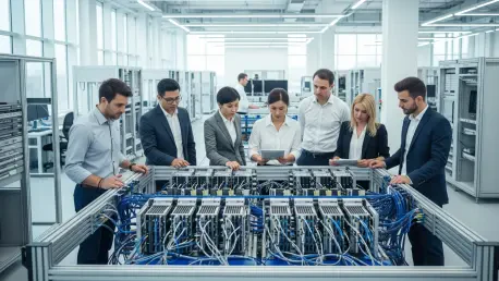
The environment has shifted from a scrappy garage to a high-intensity engineering hub where we are now managing an 80,000-square-foot facility. Today, we have 400 people bustling through an office that houses a 2-megawatt data center, while our new 10-megawatt facility down the road in Milpitas represents our next phase of industrial scaling. We are no longer just designing on screens; we are running tokens in our lab every day and working directly with the largest AI companies in the world to fine-tune their workloads on our hardware. It is a very different world from the one where I didn’t have a pillow, but the pressure is higher than ever because we have to prove that our silicon can handle the world’s most demanding inference tasks at scale. The transition has been humbling, and while I finally have a mattress and multiple pillows, the focus remains entirely on the millions of transistors we are pushing to their absolute limit.
What is your forecast for the future of specialized AI silicon?
I believe we are entering an era where the “one-size-fits-all” approach to AI hardware will become economically unsustainable for the biggest players in the industry. As models grow more specialized and the demand for real-time inference explodes, we will see a massive shift toward “etched” solutions where the core logic of the model is baked directly into the silicon to maximize efficiency. Even giants like Google are already exploring this with projects like their Frozen v2 chip, which suggests that the industry is finally moving toward the vision we had back in 2022. Within the next few years, specialized systems won’t be seen as a niche alternative; they will be the primary engines driving the global AI infrastructure, providing the speed and cost-efficiency that general-purpose chips simply cannot match.