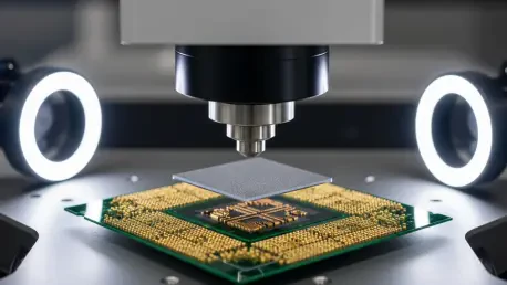

Semiconductor components have reached a level of complexity where traditional inspection methods are no longer sufficient to ensure the reliability of high-end hardware. QuantumDiamonds, a specialized spinout from the Technical University of Munich, has positioned itself at the forefront of this industrial shift by introducing quantum-based sensing solutions that address the critical bottleneck of defect identification. As the European Chips Act continues to promote technological sovereignty, the emergence of such advanced diagnostic tools is vital for maintaining a competitive edge in the global market. By utilizing synthetic diamonds to detect flaws at a microscopic level, the company provides a non-destructive alternative to traditional testing, which often requires the physical destruction of chips to verify their internal integrity. This innovation is particularly relevant as manufacturing yields become the deciding factor in the profitability of modern foundries. By accelerating the transition from laboratory research to industrial application, the startup is redefining semiconductor quality.
Securing Financial Longevity: Strategic Investments and Grants
The financial foundation of QuantumDiamonds has been significantly bolstered by a massive influx of capital, including a €76 million grant from German and Bavarian state ministries approved by the European Commission. This non-dilutive funding is a central component of a larger $178 million initiative aimed at establishing a specialized production facility in Munich for semiconductor testing equipment. Such substantial state support reflects a broader strategic interest in securing the supply chain for high-performance computing and automotive electronics. The new facility will not only serve as a manufacturing base but also as a center for research and development, ensuring that the technology continues to evolve alongside chip designs. By anchoring these operations in a major European tech hub, the company benefits from a deep pool of engineering talent and a robust network of industrial partners. This investment is a clear signal that quantum technology has moved beyond the theoretical phase into a period of intensive commercialization and scaling.
In addition to government grants, a successful €15 million equity round led by the World Fund has provided the necessary liquidity to scale international operations and meet surging market demand. This private investment highlights the growing appetite for deep tech solutions that offer immediate practical benefits to the semiconductor manufacturing sector. Global chip makers are increasingly looking for ways to integrate more efficient inspection protocols without overhauling their entire production lines. The influx of capital from the World Fund specifically supports the refinement of the hardware-software interface, allowing for faster data processing and more intuitive user experiences. Investors are particularly drawn to the scalability of the diamond-based sensing model, which can be adapted for various types of semiconductors, from power electronics to advanced memory chips. This mix of public and private funding creates a stable environment for long-term growth, allowing the company to focus on technical excellence while aggressively pursuing new market opportunities.
Diamond-Based Precision: The Mechanics of Quantum Sensing
The technological heart of the company’s solution lies in the use of synthetic diamonds to observe electricity flow at a microscopic level without interfering with the chip’s function. Traditional inspection methods, such as electron microscopy, are often limited to the surface of the component or require cross-sectioning that destroys the sample. In contrast, QuantumDiamonds utilizes the unique magnetic properties of nitrogen-vacancy centers within synthetic diamonds to perform non-destructive inspections across all layers of a chip simultaneously. This capability allows manufacturers to visualize the internal current distribution in real-time, pinpointing the exact location of shorts, leakages, or resistance anomalies. By sensing the extremely weak magnetic fields generated by moving electrons, the quantum sensors provide a level of detail that was previously unattainable outside of specialized physics laboratories. This shift toward non-invasive diagnostics is essential for maintaining high throughput in modern fabrication plants where every second of downtime translates into significant financial losses.
This breakthrough is particularly vital for the modern shift toward 3D and multi-layered architectures required for high-performance AI data centers and edge computing devices. As chips become more vertically integrated, the challenge of identifying defects hidden deep within the silicon stacks grows exponentially. Traditional optical tools cannot see through multiple layers of opaque material, but magnetic field sensing can penetrate these structures effortlessly. Quantum sensing provides a comprehensive view of the entire device, ensuring that vertical interconnects and buried layers are functioning according to design specifications. As artificial intelligence applications demand more processing power, the industry is forced to adopt these complex 3D structures, making advanced inspection tools a prerequisite for successful deployment. The ability to verify the integrity of these stacks in a matter of minutes ensures that manufacturers can iterate on new designs more quickly. This speed is a critical factor in the race to develop the most efficient and powerful processors for the next decade of computing.
Market Dominance: Economic Advantages and Global Expansion
Transitioning to quantum-based inspection offers a massive economic advantage by compressing the typical defect detection timeline from several weeks to just two minutes. This dramatic reduction in time allows foundries to identify process errors almost immediately, preventing the waste of entire wafer batches and saving hundreds of millions of dollars in material costs. The company’s business model further enhances this value proposition by pairing high-end hardware sales with a software subscription service for advanced data interpretation. This ensures that clients not only have the best sensors but also the analytical tools needed to turn raw magnetic data into actionable manufacturing insights. Currently, the startup holds a significant first-mover advantage, with no immediate equivalent competitors from the U.S. or Asia offering similar high-throughput capabilities. By implementing these systems directly on the fabrication floor, manufacturers can achieve 100% quality control, moving away from the statistical sampling methods that often allow defects to slip through to the final product.
The strategic expansion into key markets like Taiwan and Silicon Valley proved to be a decisive move in establishing the company as a global leader in semiconductor diagnostics. This aggressive scaling allowed the Munich-based team to double its engineering workforce and refine its high-throughput systems for the most demanding fabrication environments. Future considerations for the industry focused on the seamless integration of quantum sensing into fully automated “lights-out” factories, where real-time defect correction became the standard. Actionable next steps for major chipmakers involved shifting from reactive testing to proactive yield management through the deployment of diamond-based sensors across all production stages. As the technology matured, it provided a clear pathway for other quantum-driven startups to bridge the gap between academic research and large-scale industrial utility. Whether the company remained an independent powerhouse or became a strategic asset for a larger equipment provider, its role in securing the future of chip manufacturing was firmly established.